
[ China Instrument Network Instrument R&D ] Recently, the Institute of Microelectronics of the Chinese Academy of Sciences’ Integrated Circuit Pilot Process R&D Center is targeting a new generation of gate-all-around silicon nanowire (GAA SiNW) MOS devices for the 5 nanometer technology generation. New progress has been made in the research of structures and manufacturing methods.
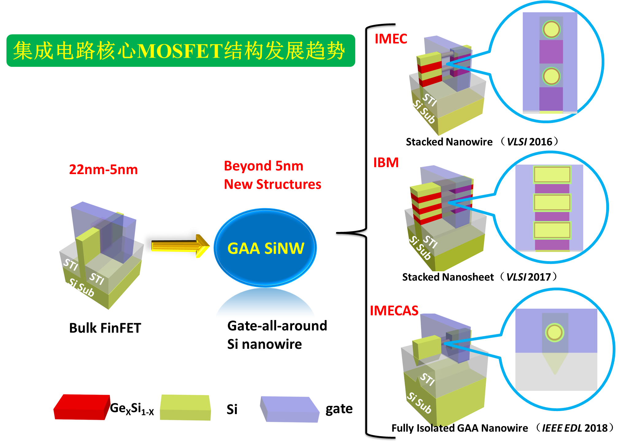
Figure 1. Trends in the Structure of Integrated Circuit Core MOS Devices
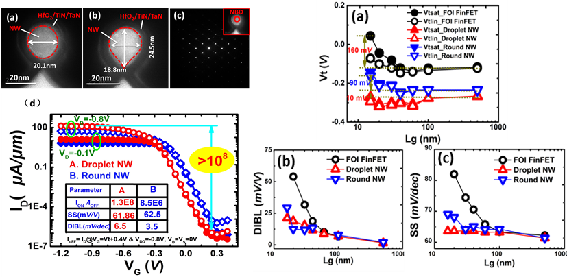
Figure 2. Structure and electrical properties of a fully isolated silicon-based gate-alloy nanowire MOSFET
Existing FinFET device structures in integrated circuit technology below 5 nanometers face many challenges. Loop-gate nanowire devices are considered to be one of the key structures that may replace FinFETs in the future due to their superiority in channel electrostatic integrity, leakage current control, and one-dimensional carrier transport of carriers. In recent years, the development of the next-generation integration technology by combining the ideal loop-gate nanowire structure with the mainstream FinFET technology has become one of the key development points for the in-depth development of integrated circuits. As shown in FIG. 1, there are currently two internationally reported research and development schemes for forming stacked nanowire devices based on the mainstream high-k metal gate FinFET manufacturing process: stacked nanowires (SNW, IMEC) and stacked nanosheets (Nanosheet, IBM) technology. . The above solutions all need to epitaxially grow a high-quality multilayered GeSi/Si structure on a common silicon substrate, and selectively etch GeSi or Si in a high-k metal gate replacement gate process, and finally select and form a stacked nanowire in the channel to be sourced. The Fin structure is maintained in the drain. This technology has many potential challenges in the large-scale manufacturing of integrated circuits: A multilayered GeSi/Si epitaxial layer with high quality, close to bulk silicon quality, must be grown; due to the introduction of Ge elements in the first integration step, the subsequent process zone Lower process temperature window limits and more Ge atom contamination opportunities.
In response to the above-mentioned challenges faced by the nanowire transistor architecture in the development of integrated circuits, the team led by Yin Huaxiang, a researcher at the Institute of Microelectronics, proposed to form bulk silicon-insulated silicon Fin and high-k through advanced etching technology based on the mainstream silicon-based FinFET integration process. The selective etching of SiO2 in the metal gate replacement gate process is combined to form a new method for fully isolating silicon-based gated nanowire MOS devices. After the insulating Fins in the replacement gate is released, the isolated "polygonal silicon Fin" is converted into two types of nanowire structures, "falling drop-shaped" and "circular" by the two processes of oxidation and hydrogen annealing. Because in this method, the nanowire channel is formed by a single crystal silicon substrate, the material in the conductive channel has fewer lattice defects and higher interface quality. Two kinds of high-k metal ring-gate nanowire transistors all exhibit good device characteristics, in which the “drop-droplet-shaped†ring-gate nanowire transistors prepared by oxidation are obtained at a physical gate length of 16 nm (corresponding to 5 nm and below). The device has subthreshold characteristics of SS = 61.86 mV/dec and DIBL = 6.5 mV/V, and the current-switching ratio is greater than 1E8. SS and DIBL are very close to the MOSFET's theoretical limit values ​​(60mV/dec and 0mV/V), far exceeding the performance parameters of FinFETs manufactured by similar processes in the past, and reaching the highest levels reported by similar devices. At the same time, this type of device structure can also be fabricated into multi-layered stacked nanowires in a multi-step etching and replacement gate process by the same method, and this research work is ongoing. This kind of manufacturing method that is different from the existing international reports has completely independent intellectual property rights and can provide various options for core device architecture and manufacturing process development for future innovation and development of the next generation of ICs in China. The work was published in the IEEE Electronic Device Letters, a new type of p-type loop-gate nanowire field effect transistor with excellent short channel control capability through an advanced process. , DOI: 10.1109/LED.2018.2807389) and was selected as the first paper in this issue.
The study was funded by the National Science and Technology Major Project 02 Special Project and the National Key R&D Program.
(Title: Microelectronics has made progress in the research of new silicon-based gated nanowire MOS devices)
K Series Shape Molding Machine
Eps Foam Box Machine,Thermocol Box Machine,Eps Decoration Product Machine,High Configuration Eps Machine
Zhejiang Huasheng Machinery Equipment Co.,Ltd , https://www.huashengepsmachine.com